What Is UCIe? The Open Standard for Chiplet Interconnects
UCIe is an open standard for wiring chiplets from different vendors into one package, defining the physical layer, protocols, and packaging it needs.
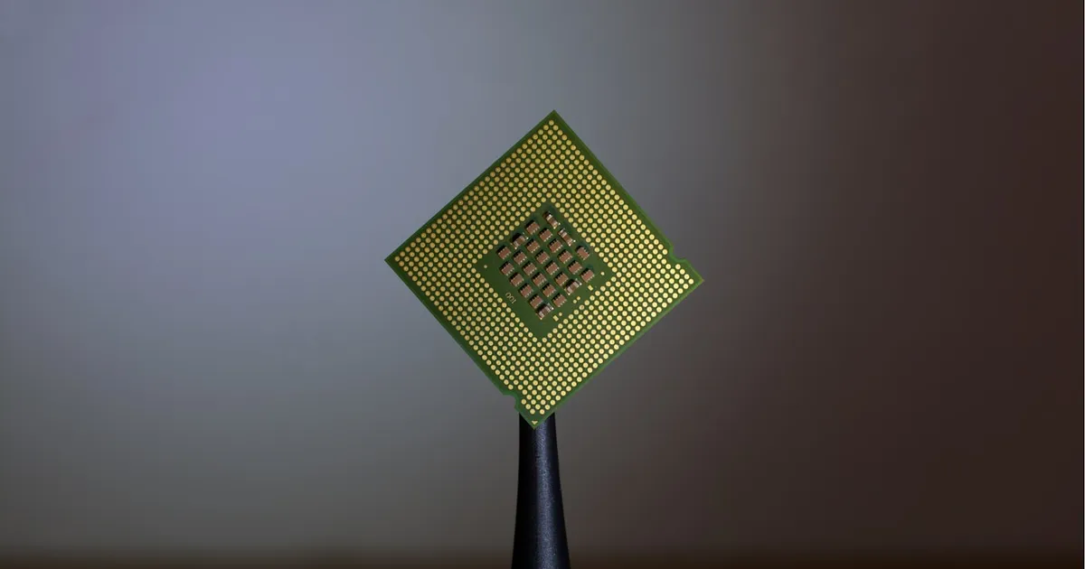
UCIe (Universal Chiplet Interconnect Express) is an open industry standard that defines how separate silicon dies — chiplets — communicate with each other inside the same chip package. It specifies the physical layer, the protocol layer, and the packaging requirements needed for a chiplet made by one company to talk reliably to a chiplet made by another, turning chiplet-based design from a collection of proprietary, single-vendor interconnects into an interoperable ecosystem.
Why chiplets need a standard at all
Modern processors increasingly aren’t a single piece of silicon. Instead of manufacturing one large monolithic die, chipmakers split the design into smaller chiplets — a compute chiplet, an I/O chiplet, memory controllers, and so on — and package them together as one logical chip. This improves manufacturing yield (smaller dies have fewer defects per unit), lets each chiplet use the best-suited process node for its job, and makes it possible to mix and match components across product generations.
The catch is that chiplets need an extremely fast, low-latency link between them to behave like a single chip rather than a collection of parts talking over a slow bus. Before UCIe, each major chipmaker built its own proprietary die-to-die interconnect — fast within one company’s product line, but incompatible with anyone else’s. UCIe, backed by a broad industry consortium, exists to replace that fragmentation with a common specification so chiplets from different vendors and different foundries can be combined in one package.
The two layers UCIe defines
UCIe’s specification splits into two main pieces, similar in spirit to how networking protocols separate physical transmission from logical framing:
- Physical layer — defines the electrical signaling, the bump pitch (the spacing of the physical connection points between dies), and the packaging options used to route signals between chiplets. UCIe supports both a standard package option, for lower-cost, longer-reach connections on an organic substrate, and an advanced package option, for extremely short, dense connections using techniques like silicon interposers or bridges — the kind of packaging used when chiplets sit very close together for maximum bandwidth per watt.
- Protocol layer — defines how data is framed and which upper-layer protocols ride on top of the physical link. UCIe can carry PCIe and CXL traffic directly, as well as a raw, low-overhead streaming mode intended for tightly coupled compute-to-compute links where minimizing latency matters more than protocol compatibility.
This layered design is deliberate: it lets UCIe reuse decades of investment in PCIe and CXL software and tooling for the cases where standard protocol semantics make sense, while still offering a leaner mode for the highest-bandwidth, lowest-latency links inside a package.
How UCIe relates to PCIe and CXL
It helps to place UCIe next to the interconnects it builds on. PCIe is the standard for connecting a chip to other components on a board — a GPU to a motherboard, for instance. CXL extends PCIe’s physical layer with a memory- and cache-coherent protocol, primarily for connecting a CPU to external memory or accelerators across a board or even between servers. UCIe operates at a different scale than both: it’s for connections within a single package, between dies that are millimeters apart rather than centimeters or meters. You can think of the three as concentric rings — UCIe for die-to-die, PCIe for board-level device connections, and CXL for coherent memory expansion — with UCIe explicitly designed to interoperate with the other two rather than compete with them.
What interoperability actually buys the industry
The practical promise of UCIe is a chiplet marketplace: a company designing a processor could, in principle, license a compute chiplet from one vendor, an I/O chiplet from another, and a specialized accelerator from a third, and combine them in one package because they all speak the same die-to-die protocol. That’s a significant shift from the current reality, where most chiplet-based products still combine chiplets designed in-house by a single company, because compatibility can’t be assumed across vendors without a shared standard.
This mirrors, at the hardware level, a familiar pattern from software: standardizing an interface (like REST did for web APIs) unlocks composability that proprietary, incompatible approaches never could. A standard die-to-die interconnect is what makes mixing chiplets from different vendors a realistic engineering plan rather than a one-off integration project.
What it means for performance and cost
Beyond interoperability, UCIe’s bandwidth-per-millimeter and power-per-bit targets are central to why the standard exists at all. Die-to-die links inside a package can achieve far higher bandwidth density and lower energy cost per bit than any off-package connection, because signals travel a much shorter distance and don’t have to cross a board-level connector. That efficiency is a big part of why chiplet designs have become attractive for high-performance processors and AI accelerators: splitting a design into chiplets only pays off if the interconnect between them doesn’t become the new bottleneck, and that’s precisely the gap UCIe is meant to close.
The takeaway
UCIe is to chiplets what standardized board-level buses were to discrete components: a common physical and protocol layer that lets pieces built by different vendors work together inside the same package. It sits below PCIe and CXL in scope — die-to-die rather than board-to-board or server-to-server — but interoperates with both, carrying their traffic when compatibility matters and offering a leaner streaming mode when raw bandwidth and latency matter more. As chiplet-based design becomes the norm for high-performance processors, a shared interconnect standard is what keeps that shift from fragmenting into as many incompatible ecosystems as there are chipmakers.
Tagged
Keep reading
 Chisato · · 4 min read
 Wafer-Scale Integration Explained
Wafer-scale integration builds one giant chip from an entire silicon wafer instead of cutting it into dies. How it works and its tradeoffs.
Chisato · · 4 min read What Is Semiconductor Yield?
Yield is the share of chips on a wafer that work. It's the single biggest driver of chip cost, and why new process nodes start out expensive.
 Chisato · · 5 min read
 2.5D vs 3D Chip Packaging Explained
2.5D packaging places dies side by side on an interposer; 3D packaging stacks dies vertically through silicon vias. How advanced packaging works.