FinFET vs Gate-All-Around (GAA) Transistors Explained
FinFETs wrap the gate around three sides of a fin; gate-all-around transistors wrap it fully around stacked nanosheets. How they differ and why it matters.
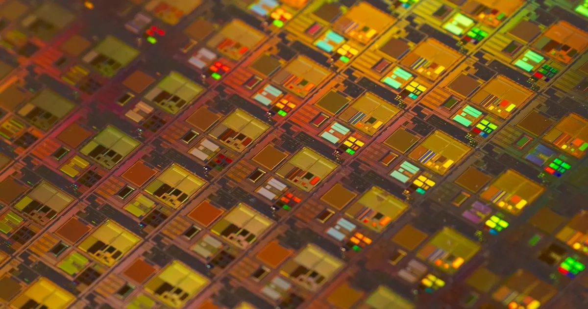
FinFET and gate-all-around (GAA) are two generations of transistor structure used in advanced logic chips. In a FinFET, the transistor’s channel is a thin vertical fin of silicon, and the gate wraps around three of its sides. In a GAA transistor, the channel is split into thin horizontal sheets or wires stacked on top of each other, and the gate surrounds each one completely. Wrapping the gate around more of the channel gives it tighter control over current, which reduces leakage and allows continued shrinking. That is why leading-edge manufacturers have been moving from FinFETs to GAA designs.
Why gate control matters
A transistor is a switch. A voltage on the gate turns current through the channel, between source and drain, on or off. The better the gate controls the channel, the more cleanly the switch turns off and the less current leaks when it should be idle.
As transistors shrink, the source and drain get closer together and begin to influence the channel themselves. These short-channel effects make the switch leaky and harder to turn off. Leakage wastes power even when a circuit is doing nothing, and it limits how far supply voltage can drop. The end of easy voltage scaling, described in our explainer on Dennard scaling, made leakage one of the central problems in chip design.
The fix, repeatedly, has been to give the gate more surface area against the channel.
Planar transistors: gate on one side
For decades, transistors were planar: the channel was a flat region at the surface of the silicon, and the gate sat on top of it. The gate only touched one side of the channel. Below it, the channel connected to the bulk silicon, giving leakage a path the gate could not fully shut off. Eventually planar transistors could not be shrunk further without unacceptable leakage.
FinFET: gate on three sides
The FinFET raised the channel into a narrow vertical fin. The gate drapes over the fin like a saddle, contacting the top and both sides. Three sides of control instead of one made a large difference, and FinFETs became the standard structure for leading-edge logic for many process generations.
FinFETs have a characteristic constraint: fin quantization. Each fin has a fixed width and height set by the process. To make a transistor stronger, meaning able to drive more current, designers add more fins. Drive strength therefore comes in integer steps: one fin, two fins, three fins. That limits fine-grained trade-offs between performance, power, and area in standard cell libraries.
As fins get thinner and taller to keep pace with scaling, they also become harder to manufacture uniformly, and the bottom of the fin remains less controlled than the rest.
Gate-all-around: gate on every side
A GAA transistor turns the channel on its side and slices it into layers. The most common form uses nanosheets: thin, wide horizontal ribbons of silicon stacked vertically, with the gate material filling the space between and around every sheet. Each sheet is surrounded on all four sides, giving the gate the strongest possible electrostatic control.
Key advantages:
- Lower leakage at small dimensions. Complete wrap-around control suppresses short-channel effects better than three-sided control.
- Tunable width. Designers can choose nanosheet width as a continuous parameter rather than adding whole fins, breaking the fin quantization constraint. Wider sheets give more drive current; narrower sheets save area and power.
- More current per footprint. Stacking several sheets vertically increases the effective channel width without growing the transistor’s footprint on the wafer.
- Lower operating voltage. Better control lets circuits switch reliably at lower voltages, which reduces dynamic power.
Different manufacturers use different trade names for their nanosheet transistors, but the underlying structure is the same idea.
FinFET vs GAA at a glance
| Planar | FinFET | Gate-all-around (nanosheet) | |
|---|---|---|---|
| Channel shape | Flat surface region | Vertical fin | Stacked horizontal sheets |
| Gate contact | One side | Three sides | All sides of each sheet |
| Leakage control | Weakest | Strong | Strongest |
| Drive-strength tuning | Continuous width | Integer number of fins | Continuous sheet width plus sheet count |
| Manufacturing complexity | Lowest | High | Higher |
| Status | Mature and trailing-edge nodes | Workhorse of many advanced nodes | Leading-edge nodes |
How GAA transistors are built
Manufacturing nanosheets is considerably harder than manufacturing fins. A simplified outline:
- Grow a superlattice. Alternating layers of silicon and silicon-germanium are grown epitaxially, forming a stack.
- Pattern the stack into fin-like columns, much as in a FinFET process.
- Form inner spacers. The silicon-germanium layers are partially recessed at the edges and filled with insulating spacers that separate the future gate from the source and drain.
- Release the sheets. A highly selective etch removes the remaining silicon-germanium, leaving silicon sheets suspended between the source and drain.
- Wrap the gate. Gate dielectric and metal are deposited into the gaps so they surround every sheet.
Each step demands extreme precision at the atomic scale. These processes rely on advanced patterning, including EUV lithography, and on tight control of deposition and etching. Variations from sheet to sheet can affect performance, which feeds into how chips are sorted through binning.
What comes after nanosheets
GAA is not the end of the roadmap. Researchers and manufacturers have described several follow-on ideas:
- Forksheet transistors place n-type and p-type nanosheet stacks side by side with a thin dielectric wall between them, letting the two sit closer together.
- Complementary FET (CFET) stacks an n-type transistor directly on top of a p-type one, potentially cutting the footprint of basic logic cells substantially.
- Backside power delivery moves power wiring beneath the transistors, freeing the front side for signal routing. It is independent of transistor shape but often discussed alongside GAA because the two arrive at similar points on roadmaps.
Transistor architecture is also only one lever. Node names no longer correspond to any physical dimension, as our guide to semiconductor process nodes explains, and much of today’s performance scaling comes from packaging approaches such as chiplets.
The takeaway
FinFETs wrap the gate around three sides of a vertical fin; gate-all-around transistors wrap it fully around stacked horizontal nanosheets. That extra control reduces leakage, allows lower voltages, and lets designers tune transistor width continuously instead of in whole-fin steps. The cost is a much harder manufacturing process. GAA is the current step in a long progression from planar to FinFET, with stacked designs like CFET already being explored as the next one.
Tagged
Keep reading
 Chisato · · 4 min read
Wafer-Scale Integration Explained
Wafer-scale integration builds one giant chip from an entire silicon wafer instead of cutting it into dies. How it works and its tradeoffs.
Chisato · · 4 min read What Is Semiconductor Yield?
Yield is the share of chips on a wafer that work. It's the single biggest driver of chip cost, and why new process nodes start out expensive.
 Chisato · · 5 min read
2.5D vs 3D Chip Packaging Explained
2.5D packaging places dies side by side on an interposer; 3D packaging stacks dies vertically through silicon vias. How advanced packaging works.