What Is Dennard Scaling? Why Clock Speeds Stopped Climbing
Dennard scaling held that shrinking transistors kept power density constant, letting clock speeds rise for free. Its breakdown reshaped chip design.
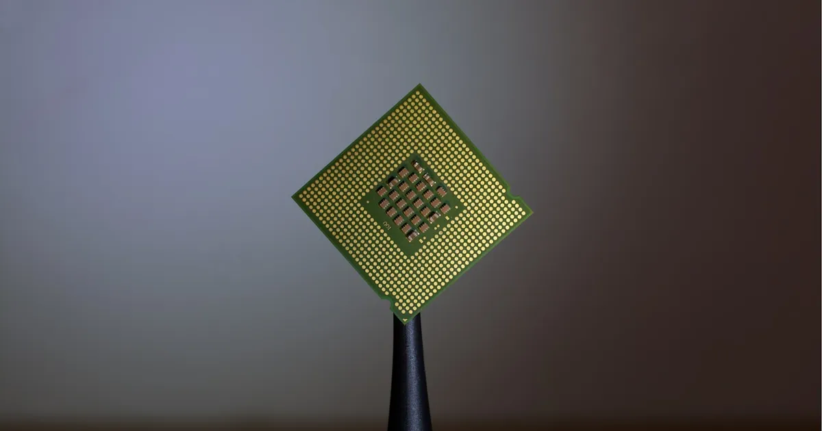
Dennard scaling is the observation, formalized by Robert Dennard and colleagues in 1974, that as transistors shrink, their voltage and current shrink proportionally too — so power density (power per unit area) stays roughly constant even as transistor count on a chip goes up. For decades that meant each new, smaller process node could run at a higher clock speed within the same power and cooling budget. When Dennard scaling broke down in the mid-2000s, it forced the entire chip industry to change strategy, and the effects of that shift are still visible in every processor sold today.
What the scaling relationship actually says
Dennard’s insight, distinct from Moore’s law, was about how smaller transistors behave, not just how many fit on a chip. Moore’s law predicts that transistor density roughly doubles on a regular cadence. Dennard scaling predicted something additional: if you shrink a transistor’s linear dimensions by a factor and scale its voltage down by the same factor, its power consumption drops by the square of that factor, while its switching speed increases. Put those together, and power density — power divided by the shrinking area — stays flat.
That was the free lunch of chip design for roughly three decades: every process shrink gave you more transistors, each one individually faster and lower-power, without the chip getting hotter per square millimeter. Clock speeds could rise year over year largely because the power budget allowed it.
To see why that follows, imagine shrinking every linear dimension of a transistor by half while also halving its operating voltage. Capacitance drops with size, and the power a transistor draws while switching falls with the square of voltage, so despite packing four times as many transistors into the same area, total power on that area stays about the same. Switching speed goes up as dimensions shrink too, so the natural result is a chip that runs faster, does more work, and generates the same heat per square millimeter as its predecessor — which is exactly the trend clock speeds followed through the 1990s and early 2000s.
Why it broke down
Dennard scaling assumed voltage could keep shrinking alongside transistor size. In practice, voltage couldn’t keep falling below a certain point without leakage current — current that flows even when a transistor is nominally “off” — starting to dominate power consumption. Leakage doesn’t scale down the way switching power does; below roughly the 90 nanometer node, it became a large and growing share of total chip power, which broke the assumption that power density stays constant.
The result, visible in chip roadmaps from the mid-2000s onward, was that clock speeds essentially plateaued in the low single-digit gigahertz range, even as transistor counts kept climbing under Moore’s law. Adding more transistors was still possible; running them all significantly faster, for free, was not.
How the industry responded
Chipmakers couldn’t keep raising clock speed, so they redirected the transistor budget elsewhere:
- More cores, not faster cores. Rather than one core running faster, chips added multiple cores running at similar clock speeds, trading single-thread speed increases for parallel throughput. This is the shift that made multi-core CPUs, and eventually manycore GPUs, the default rather than the exception.
- Deeper microarchitecture, not just higher frequency. Techniques like wider out-of-order execution windows, better branch prediction, and more aggressive instruction pipelining squeeze more work out of each clock cycle instead of raising the cycle rate itself — the same reasoning behind why IPC matters as much as clock speed for real-world performance.
- Power and clock gating. Since leakage from idle transistors became a bigger share of the power budget, chips started aggressively shutting off power (power gating) or clock signals to unused circuit blocks rather than leaving them powered but idle.
- Specialization. If general-purpose cores can’t get dramatically faster for free, dedicating silicon area to fixed-function accelerators — for video decode, cryptography, or AI inference — became a more attractive way to spend a growing transistor budget than making the general-purpose core marginally faster.
- Thermal management as a first-class constraint. Thermal throttling — dynamically reducing clock speed when a chip runs too hot — became a standard part of chip operation rather than an edge case, precisely because power density is no longer something a smaller process node keeps in check automatically.
Dennard scaling vs. Moore’s law
| Moore’s law | Dennard scaling | |
|---|---|---|
| What it predicts | Transistor count roughly doubles per node | Power density stays constant as transistors shrink |
| Status today | Slowing, but still broadly continuing | Broke down in the mid-2000s |
| Main consequence when active | More transistors per chip | Higher clock speeds for free |
| What replaced it | Continued density gains via new techniques (3D stacking, new materials) | Multi-core, wider pipelines, specialization, power gating |
Why this still matters
Every design decision behind simultaneous multithreading, the shift toward heterogeneous cores that pair high-performance and high-efficiency designs on the same die, and the general industry pivot toward domain-specific accelerators over the last two decades traces back to the same root cause: transistors kept getting smaller and more numerous, but they stopped getting proportionally more power-efficient at a fixed voltage. Understanding Dennard scaling’s breakdown explains why “just raise the clock speed” stopped being a viable performance strategy, and why chip design since has been about extracting parallelism and specialization instead.
The takeaway
Dennard scaling described a relationship, not a law of physics that had to hold forever: shrink a transistor, shrink its voltage proportionally, and power density stays flat — letting clock speeds rise for free with every process node. Once voltage stopped scaling down around the 90 nanometer node, that free lunch ended, and the industry pivoted from raw frequency to cores, pipeline depth, gating, and specialization to keep performance climbing within a fixed power and thermal budget.
Keep reading
 Chisato · · 4 min read
 What Is HBM? High Bandwidth Memory Explained
HBM stacks DRAM dies vertically and connects them through a wide interface, trading capacity per chip for far higher bandwidth than standard DRAM.
 Chisato · · 5 min read
 What Is Simultaneous Multithreading (SMT)?
Simultaneous multithreading lets one physical CPU core run two instruction streams at once, filling idle execution units to raise throughput.
Chisato · · 4 min read Thermal Interface Materials Explained
Thermal interface material fills microscopic gaps between a chip and its heatsink so heat can actually transfer to the cooler.