What Is HBM? High Bandwidth Memory Explained
HBM stacks DRAM dies vertically and connects them through a wide interface, trading capacity per chip for far higher bandwidth than standard DRAM.
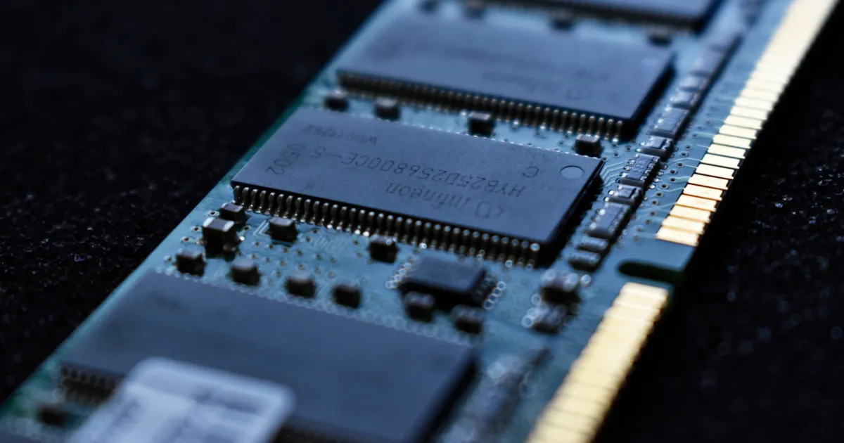
High Bandwidth Memory, or HBM, is a type of DRAM built by stacking multiple memory dies vertically and connecting them to a processor through a very wide interface, rather than the narrow, long traces that connect conventional DRAM modules to a CPU. The result is dramatically higher data throughput per package, at the cost of higher manufacturing complexity and lower capacity per chip than standard memory.
HBM exists to solve a specific bottleneck: modern GPUs and AI accelerators can perform far more calculations per second than conventional memory can feed them data. If memory bandwidth can’t keep up with compute, expensive processing units sit idle waiting on data. HBM is the industry’s answer to that gap.
How HBM differs physically from standard DRAM
Conventional DRAM — the kind used in most laptops and servers, like DDR modules — sits on a separate module connected to the processor over a relatively narrow bus, often 64 bits wide per channel, running at very high clock speeds to compensate.
HBM takes the opposite approach: instead of a few very fast, narrow connections, it uses an extremely wide interface — often 1,024 bits per stack — running at more modest clock speeds. It achieves its bandwidth through parallelism rather than raw frequency.
To make that wide interface physically possible, HBM stacks several DRAM dies directly on top of each other, connected vertically through through-silicon vias (TSVs) — microscopic vertical electrical connections drilled through the silicon itself. This stack sits on an interposer, a silicon substrate that also holds the processor (GPU or accelerator), placing memory and compute extremely close together. That physical proximity is what makes the wide interface practical: routing a thousand-plus signal lines any real distance would be impossible with conventional circuit board traces.
This is a related but distinct idea from 2.5D and 3D chip packaging more broadly — HBM is one of the most common real-world applications of that packaging approach, using an interposer to place memory and logic dies side by side or stacked, connected by extremely short, dense wiring instead of a traditional circuit board.
Why it matters for AI and graphics workloads
GPUs and AI accelerators process enormous amounts of data in parallel — reading weights, activations, and intermediate results from memory continuously during training and inference. If the memory subsystem can’t supply data fast enough, the compute cores stall, and expensive silicon does nothing but wait.
HBM’s wide-and-parallel design gives it far more aggregate bandwidth than a comparable footprint of conventional DRAM. That’s why nearly every modern AI training and inference accelerator ships with HBM stacks mounted directly next to the compute die, rather than routing to memory across the board the way a typical CPU does with its RAM.
HBM vs GDDR vs standard DRAM
Graphics cards have historically used GDDR, a different high-speed DRAM variant, rather than either standard DRAM or HBM. It’s worth knowing where each fits.
| Standard DRAM (DDR) | GDDR | HBM | |
|---|---|---|---|
| Interface width | Narrow (e.g. 64-bit per channel) | Moderate, higher clocked | Very wide (1,024-bit+ per stack) |
| Physical placement | Separate module/slot | On-board, near the GPU | Stacked directly on an interposer with the processor |
| Bandwidth per package | Lowest | Middle | Highest |
| Capacity per package | Highest, easily expandable | Moderate | Lower, fixed at manufacture |
| Manufacturing cost | Lowest | Moderate | Highest — requires interposers and TSV stacking |
| Typical use | General-purpose computing, servers | Consumer/gaming GPUs | AI accelerators, data-center GPUs, HPC |
GDDR is a middle ground: cheaper and easier to manufacture than HBM, with more bandwidth than standard DDR, which is why it remains the default for consumer graphics cards. HBM’s cost and complexity are only worth paying when bandwidth is the binding constraint and the workload can tolerate — or work around — its more limited capacity per package.
The tradeoffs
HBM isn’t a strict upgrade over other memory types. Its downsides are real:
- Capacity. Because dies are stacked and space-constrained, a given HBM package holds less data than an equivalent footprint of standard DRAM modules. Accelerators compensate by using multiple HBM stacks side by side, but total capacity is still typically far below what a server’s main memory offers.
- Cost. TSV stacking and interposer packaging are expensive and yield-sensitive processes compared to producing standard DRAM chips. This cost gets passed directly into the price of HBM-equipped hardware.
- Repairability and flexibility. HBM is soldered directly into the package at manufacture time, unlike DIMM-based DRAM, which can be added, removed, or upgraded after the fact.
These tradeoffs are exactly why HBM shows up in accelerators and high-performance computing rather than general-purpose servers or consumer PCs — the workloads that need it are bandwidth-bound and can justify the cost, while everyday computing is better served by cheaper, higher-capacity, swappable DRAM.
The takeaway
HBM solves the memory bandwidth bottleneck that starves modern AI and graphics accelerators, by stacking DRAM dies vertically and wiring them through an extremely wide interface placed physically next to the compute die. It trades capacity, cost, and flexibility for bandwidth that conventional DRAM and even GDDR can’t match, which is exactly the trade that data-center AI hardware is built around — bandwidth is usually the scarcer resource, and HBM is the industry’s most direct answer to that scarcity.
Keep reading
 Chisato · · 4 min read
 What Is Dennard Scaling? Why Clock Speeds Stopped Climbing
Dennard scaling held that shrinking transistors kept power density constant, letting clock speeds rise for free. Its breakdown reshaped chip design.
Chisato · · 5 min read What Is Simultaneous Multithreading (SMT)?
Simultaneous multithreading lets one physical CPU core run two instruction streams at once, filling idle execution units to raise throughput.
Chisato · · 4 min read Thermal Interface Materials Explained
Thermal interface material fills microscopic gaps between a chip and its heatsink so heat can actually transfer to the cooler.