Wafer-Scale Integration Explained
Wafer-scale integration builds one giant chip from an entire silicon wafer instead of cutting it into dies. How it works and its tradeoffs.
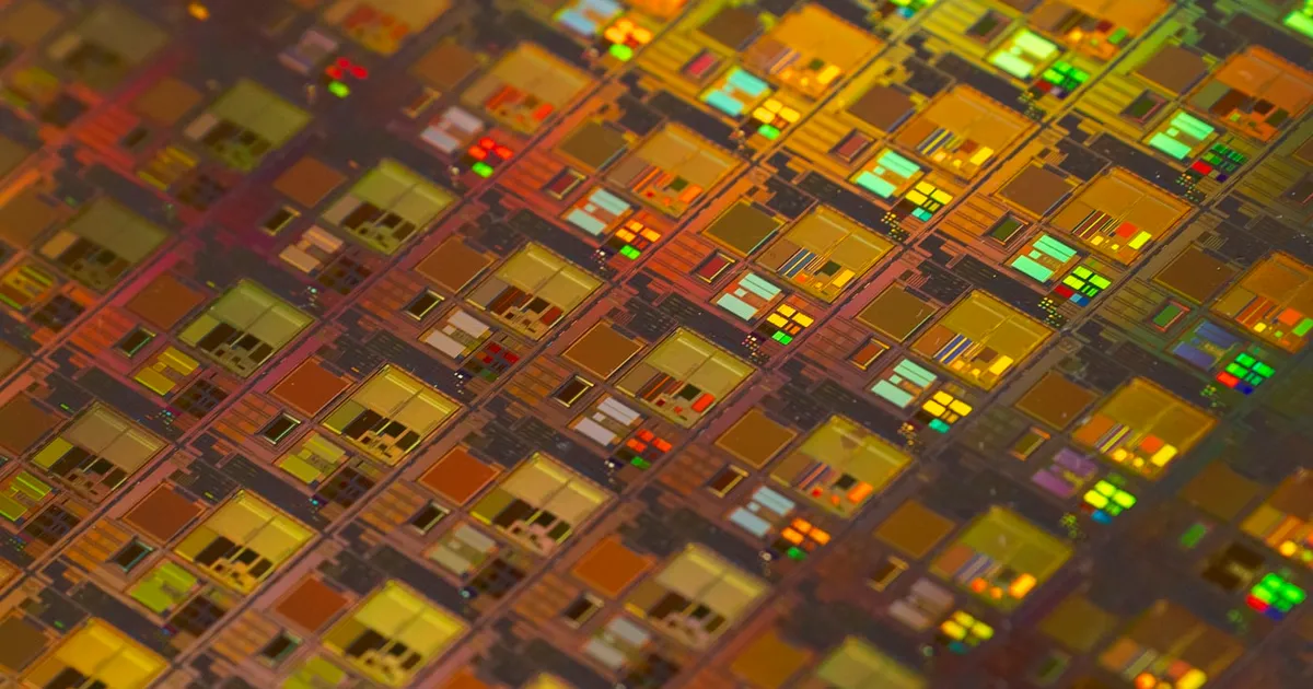
Wafer-scale integration is a chip manufacturing approach that treats an entire silicon wafer as a single functional device, instead of cutting it into hundreds of individual dies. Rather than dicing the wafer and packaging each die separately, the interconnects between what would normally be separate chips are etched directly across the wafer, producing one enormous piece of silicon with far more transistors, cores, and on-chip memory than any single reticle-limited die could hold.
How normal chip manufacturing works, for contrast
In conventional manufacturing, a silicon wafer is patterned with many identical copies of a chip design, limited in size by the reticle limit — the maximum area a lithography system can expose in one pass, roughly 850 square millimeters with current tools. After fabrication, the wafer is tested, cut apart with a saw, and each surviving die is packaged individually. Dies that fail testing (due to defects that land within their boundaries) are discarded — see semiconductor yield for how that discard rate is measured and why it matters economically.
Wafer-scale integration skips the cutting step. The whole wafer — often 300mm in diameter, tens of thousands of square millimeters — stays intact as one chip, with the routing between what would have been separate reticle tiles fabricated as first-class interconnect rather than left for packaging to stitch back together afterward.
Why this is hard: the defect problem
The reticle limit exists for practical reasons, and the biggest one is yield. Silicon wafers inevitably contain manufacturing defects distributed roughly randomly across their surface. A small die has a good chance of landing entirely on a defect-free patch of silicon; a chip covering the whole wafer is nearly guaranteed to overlap at least one flaw somewhere.
Traditional wafer-scale designs floundered on exactly this problem for decades — a single defect could kill the whole (very expensive) wafer. Modern approaches solve it with redundancy: the design is built from many identical small compute tiles connected by a fault-tolerant fabric, and if a defect lands on one tile, that tile — and only that tile — is routed around and disabled. The rest of the wafer keeps working. This turns what used to be a catastrophic yield problem into a tolerable loss of a small fraction of total compute capacity.
Why build a chip this big
The appeal is bandwidth and integration density. Every boundary between chips — even chips sitting a few millimeters apart on the same interposer, as in 2.5D and 3D packaging — costs latency, energy, and bandwidth compared to keeping a signal on-die. A wafer-scale chip eliminates the chip-to-chip hop almost entirely for the compute it contains: cores that would otherwise sit on separate packages, connected by comparatively slow and power-hungry off-chip links, sit on the same continuous piece of silicon instead. That translates into dramatically more on-chip SRAM and far higher aggregate memory bandwidth than assembling the equivalent compute from discrete chips connected over a board.
This matters most for workloads that are bottlenecked on moving data between compute units rather than on raw arithmetic throughput — large-scale AI training and inference being the leading example, which is why wafer-scale designs have found their niche there rather than in general-purpose computing.
The tradeoffs
Wafer-scale integration isn’t a free upgrade; it trades away flexibility and cost efficiency that reticle-sized chips take for granted:
- Cost per wafer is much higher. You can’t sell partially-defective output as a smaller, cheaper part the way you can bin a normal die (see chip binning) — the whole wafer is one product.
- Cooling and power delivery become engineering problems in their own right. Delivering even power and removing heat evenly across an entire wafer’s surface, rather than a postage-stamp-sized die, requires custom packaging and cooling infrastructure that doesn’t exist off the shelf.
- It only pays off at a specific scale. For workloads that fit comfortably on a handful of conventional chips connected by NVLink or PCIe, the complexity of wafer-scale manufacturing isn’t worth it. It makes economic sense specifically when the alternative is stitching together dozens or hundreds of discrete chips with all the interconnect overhead that implies.
- Manufacturing is inflexible. A defect in the fabric connecting redundant tiles — rather than in a tile itself — is a much harder failure mode to route around, so the redundancy scheme has to be designed in from the start.
Where it fits relative to other scaling strategies
Wafer-scale integration sits at one extreme of a spectrum of ways to pack more compute into a system. At the other end is simply connecting more discrete chips, as in a CPU-vs-GPU-vs-TPU cluster networked over standard interconnects. In between sit chiplet-based designs, where a handful of smaller dies (see what a chiplet is) are packaged together on an interposer to get some of the density benefit of monolithic integration without inheriting the yield risk of covering a full wafer. Wafer-scale integration is the logical endpoint of that trend, made viable only by aggressive redundancy and by process nodes mature enough (see semiconductor process nodes) to keep defect density low enough to tolerate.
The takeaway
Wafer-scale integration builds a single chip out of an entire silicon wafer instead of dicing it into individual dies, eliminating the chip-to-chip interconnect bottleneck for workloads that need enormous on-chip memory and bandwidth. The historical blocker was yield — one defect could kill an entire wafer — and it’s solved today with tile-level redundancy that routes around bad regions rather than discarding the whole part. It’s a specialized, expensive approach that makes sense for data-hungry workloads like large-scale AI, not a general replacement for conventional reticle-sized chips connected by packaging or networking.
Tagged
Keep reading
 Chisato · · 4 min read
 What Is Semiconductor Yield?
Yield is the share of chips on a wafer that work. It's the single biggest driver of chip cost, and why new process nodes start out expensive.
 Chisato · · 5 min read
 2.5D vs 3D Chip Packaging Explained
2.5D packaging places dies side by side on an interposer; 3D packaging stacks dies vertically through silicon vias. How advanced packaging works.
Chisato · · 4 min read How Computer Chips Are Made: Wafer to Package
Chip fabrication turns a silicon wafer into a working processor through photolithography, etching, doping, and packaging — here's the full process.