DDR4 vs DDR5: What Actually Changed
DDR5 raises transfer rates, splits each module into two independent sub-channels, and moves voltage regulation onto the module itself. Here's what that buys you.
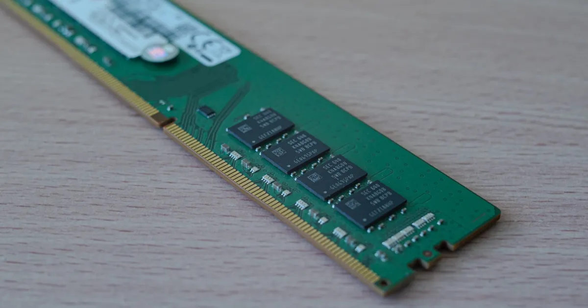
DDR5 is the JEDEC standard that succeeds DDR4 as mainstream system memory, and the jump between them is bigger than a routine speed bump. DDR5 raises baseline transfer rates well beyond DDR4’s ceiling, splits every module into two independently addressable sub-channels instead of one, and moves voltage regulation from the motherboard onto the memory module itself. Together, those changes target both raw bandwidth and the kind of fine-grained access patterns that modern multi-core CPUs actually generate.
Same underlying technology, different generation
Both DDR4 and DDR5 are forms of DRAM — synchronous dynamic RAM that stores each bit as a charge in a capacitor and requires periodic refreshing. DDR5 isn’t a different technology so much as a redesign of how that same storage is organized, clocked, and delivered to the CPU, in the same way each prior DDR generation reworked the previous one rather than replacing the underlying cell design.
The sub-channel split
The single biggest architectural change is that a DDR5 module splits into two independent 32-bit sub-channels, where a DDR4 module operates as one 64-bit channel. Each DDR5 sub-channel handles its own requests independently, with its own command and address signals. In practice, this means a DDR5 module can service two separate memory requests more efficiently than a DDR4 module handling the same traffic as one wider channel — a meaningful win for multi-core CPUs issuing many small, unrelated memory accesses at once, which is closer to how real workloads actually behave than one continuous stream of sequential reads. This is the same underlying motivation covered in single vs. dual vs. quad-channel memory: more independent paths to memory generally beats one wider shared path when access patterns are unpredictable.
Voltage regulation moves onto the module
DDR4 relies on the motherboard to regulate the voltage delivered to memory. DDR5 moves that job onto the module itself, via an onboard power management IC. This gives each module tighter, more consistent voltage regulation independent of motherboard design quality, and it’s part of why DDR5 operates at a lower standard voltage than DDR4 — lower voltage generally means lower power draw per unit of bandwidth delivered, which matters as transfer rates climb.
On-die ECC: reliability, with a caveat
DDR5 introduces on-die error-correcting code as a standard feature, where DDR4 required dedicated ECC modules to get any error correction at all. It’s worth being precise about what this buys you: DDR5’s on-die ECC corrects errors that occur within the memory chip itself, as a byproduct of increasingly dense cells being more prone to bit flips at smaller process geometries. It is not the same guarantee as full end-to-end ECC memory, which also protects data in transit between the chip and the CPU. See what is ECC memory for the fuller distinction — a DDR5 system without dedicated ECC modules still lacks the transit-level protection that server workloads typically require.
Side-by-side comparison
| DDR4 | DDR5 | |
|---|---|---|
| Channel architecture | One 64-bit channel per module | Two independent 32-bit sub-channels per module |
| Standard voltage | Higher | Lower |
| Voltage regulation | On the motherboard | On the module (onboard PMIC) |
| On-die ECC | Not standard | Standard feature |
| Peak transfer rates | Lower ceiling | Substantially higher ceiling |
| Module density | Lower per-module capacity | Higher per-module capacity |
What this means for latency vs bandwidth
Raw transfer rate numbers make DDR5 look like a strict bandwidth upgrade, and it is — but bandwidth and latency are different metrics, and early DDR5 parts often carried higher raw latency (measured in clock cycles) than mature DDR4 parts, even though the higher clock speed meant the actual time-based latency was comparable or better. This is a familiar pattern at the start of any DRAM generation: the first parts prioritize hitting the new standard’s minimum bandwidth target, and lower-latency parts arrive as the process matures. It’s the same underlying trade-off covered in memory bandwidth vs. latency — a generational bandwidth increase doesn’t automatically mean every workload gets faster, particularly latency-sensitive ones that don’t saturate available bandwidth in the first place.
Should it change a buying decision
For most general-purpose systems, the memory generation is dictated by the CPU platform, not chosen independently — a given CPU socket typically supports one generation or the other, not both. Where there is a real choice, the case for DDR5 is strongest for workloads that are actually bandwidth-hungry — multi-threaded compilation, video encoding, memory-bound scientific computing, and modern GPUs’ host-side data feeding. Workloads that are latency-sensitive and don’t saturate bandwidth see a smaller practical difference, even though DDR5 is, generation over generation, still the newer and generally faster standard.
The takeaway
DDR5 improves on DDR4 with higher transfer rate ceilings, a per-module split into two independent sub-channels, onboard voltage regulation, and standard on-die ECC — changes aimed as much at serving many small unpredictable memory accesses efficiently as at raw peak bandwidth. The generational upgrade is real, but its benefit is workload-dependent: bandwidth-bound tasks see the clearest gains, while latency-sensitive tasks benefit less than the headline transfer-rate numbers suggest.
Keep reading
 Chisato · · 4 min read
 Thermal Interface Materials Explained
Thermal interface material fills microscopic gaps between a chip and its heatsink so heat can actually transfer to the cooler.
Chisato · · 4 min read Clock Speed vs. IPC: What Actually Makes a CPU Fast
Clock speed measures cycles per second; IPC measures work done per cycle. Real CPU performance is the product of both, not either one alone.
 Chisato · · 4 min read
 UMA vs NUMA: Memory Architecture Explained
UMA gives every CPU core equal-latency memory access; NUMA gives each core faster access to its local memory bank. How the two architectures differ.