What Is a Memory Controller?
A memory controller is the circuit that manages every read and write between the CPU and main memory, setting the ceiling on bandwidth and latency.
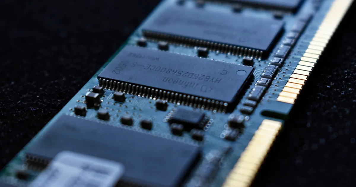
A memory controller is the piece of hardware that manages every transaction between a processor and its main memory (DRAM), translating requests from the CPU into the specific electrical signaling and timing sequences that memory chips require. Every read or write a program performs eventually passes through a memory controller — it’s the traffic director between fast, expensive on-chip logic and comparatively slow, cheap off-chip memory.
What it does
A memory controller handles a set of jobs that are invisible to software but define how fast a system actually runs:
- Address translation and mapping. It converts a physical memory address into the specific channel, rank, bank, and row/column coordinates a DRAM chip actually understands.
- Command scheduling. DRAM operations — opening a row, reading or writing a column, closing a row (precharge), refreshing — have to happen in a specific order with specific minimum delays between them. The controller schedules these commands, often reordering pending requests to minimize the number of costly row switches.
- Refresh management. DRAM cells leak charge and must be refreshed periodically or they lose their stored data. The controller issues these refresh cycles on a schedule, stealing a small amount of bandwidth to do so.
- Timing enforcement. Parameters like row-to-column delay and precharge time are fixed by the memory standard and the specific module installed; the controller enforces them so commands aren’t issued before the memory chip is actually ready.
None of this is visible to application code. A program just issues a load or store; the memory controller is what turns that into an actual sequence of electrical commands on the memory bus.
Where it sits, and why that moved
For a long time, the memory controller lived on a separate chip — the northbridge — sitting between the CPU and RAM on the motherboard, as covered in what is a northbridge/southbridge. Every memory access had to cross the bus connecting the CPU to that separate chip before it even reached memory, adding latency to every single transaction.
Modern CPUs instead integrate the memory controller directly onto the processor die. This removes an entire hop: the CPU talks to DRAM through an on-chip controller rather than routing through a separate chip first, cutting latency and letting the controller run at the CPU’s own clock domain rather than a slower shared bus. This shift is a large part of why memory latency improved even as raw DRAM cell speed improvements slowed — the controller got structurally closer to the core issuing the request.
Bandwidth, channels, and why more channels help
A single memory channel can only move so much data per cycle, set by its width and clock speed. Adding channels — separate, parallel paths to different sets of DRAM chips — multiplies available bandwidth, because the controller can issue independent commands to each channel simultaneously rather than serializing every request through one path.
This is the mechanism behind single, dual, and quad-channel memory configurations: a dual-channel setup isn’t just “two sticks of RAM instead of one,” it’s the memory controller actually splitting and interleaving traffic across two independent electrical paths, roughly doubling theoretical bandwidth. The practical benefit depends heavily on workload — see memory bandwidth vs latency for why some workloads care almost entirely about one or the other.
Memory controllers also support interleaving at a finer grain than whole channels — spreading consecutive addresses across banks so that while one bank is busy completing a row operation, the next request can already be in flight against a different, idle bank. This hides a meaningful fraction of DRAM’s inherent latency behind other in-flight work, provided the access pattern is favorable.
Memory controllers across different systems
| System type | Typical controller design | Why |
|---|---|---|
| Consumer CPU | Integrated on-die, 2-4 channels | Balances cost, bandwidth, and board complexity |
| Server CPU | Integrated on-die, 6-12+ channels | Large core counts need proportionally more bandwidth |
| GPU | Wide, high-channel-count controller for GDDR or HBM | Massively parallel workloads need far higher bandwidth than latency-sensitive CPU work |
| Multi-socket server (NUMA) | Multiple controllers, one per socket, each closer to its local memory | Avoids a single controller becoming a bottleneck as core count scales across sockets |
The controller’s design tracks what the rest of the system prioritizes. GPUs, which run thousands of threads that tolerate latency but demand throughput, pair with controllers optimized for wide, high-bandwidth memory like HBM. CPUs, which run fewer threads that are more latency-sensitive, favor controllers tuned to keep individual request latency low.
Reliability features
Server-grade memory controllers add error handling that consumer ones typically skip. ECC memory relies on the controller to compute and check error-correcting codes on every transaction, detecting and often silently correcting single-bit errors before they corrupt a running program — critical for systems where an undetected bit flip in a long-running computation is unacceptable. Some server controllers also support memory mirroring or sparing, where the controller can fail over to a redundant memory region if a DIMM starts showing correctable errors at an elevated rate, without taking the system down.
Newer interconnect standards like CXL extend what a memory controller can address beyond directly-attached DRAM, letting a CPU’s memory space span pooled or disaggregated memory connected over a CXL link rather than only DIMMs plugged directly into its own channels — effectively pushing part of the memory controller’s addressing job onto a shared, standardized interconnect.
The takeaway
The memory controller is the circuit that turns a CPU’s memory requests into the precisely-timed commands DRAM actually requires, and its design — channel count, integration on-die versus on a separate chip, reliability features — sets much of the practical ceiling on a system’s real-world memory bandwidth and latency. Moving it on-die and adding channels are the two biggest levers system designers have pulled over the years, and matching controller design to workload (latency-tuned for CPUs, bandwidth-tuned for GPUs) explains a lot of why otherwise similar-looking chips perform so differently on memory-bound work.
Tagged
Keep reading
 Chisato · · 4 min read
 What Is a DPU (Data Processing Unit)?
A DPU is a specialized chip that offloads networking, storage, and security tasks from the CPU. How data processing units fit alongside CPUs and GPUs.
Chisato · · 4 min read What Is a Semiconductor Process Node?
A process node like '5nm' or '3nm' names a chipmaker's manufacturing generation, not a literal measurement anymore. Here's what the number means.
 Chisato · · 5 min read
 RISC vs CISC: Instruction Set Architectures Explained
RISC and CISC are two philosophies for CPU instruction sets — simple fixed-length instructions versus fewer, complex ones. How they differ and why.